

이산화 주석
SnO₂증착 방식: PVD — Sputter & Evaporator
분류: 산화물
화학식: SnO₂
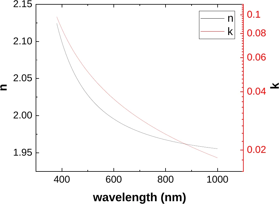
RF 마그네트론 스퍼터링으로 증착하는 이산화 주석(SnO₂) 박막입니다. 141 nm 막 기준 굴절률 1.999 @ 587 nm이며, 가스 센서·투명 전도층에 쓰이는 안정적 광대역 산화물입니다. 타깃: 순도 99.5 %, 3인치.
Specifications
Thin-Film Specifications
- Film-coated by RF magnetron sputtering vacuum < 1.0 × 10⁻⁶ Torr
- Substrate : Si (100)
- Thickness : 141 nm
- Refractive Index (n) : 1.998737 (@ 587 nm)
- Extinction Coefficient (k) : 0.03812 (@ 587 nm)
Target Specifications
- Target Material : Tin Dioxide
- Purity : 99.5%
- Diameter : 3”
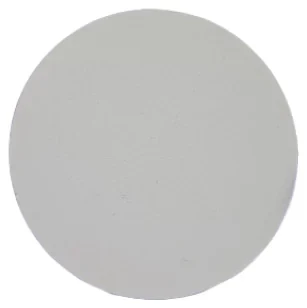 Target