


Technology
Advanced thin films
for next-generation hardware
VanaM provides process technology, custom deposition recipes, and pilot manufacturing for thin films that conventional suppliers cannot easily deliver. Our platform integrates vacuum deposition, pre/post treatment, in-situ process monitoring, metrology, and AI-assisted optimization.
Key advantages
Core IP & Novel Materials
Proprietary source and deposition know-how for high crystallinity thin films, including materials that are not yet commercialized.
Cost-Competitive Foundry
Low MOQ prototyping and small batch production reduce early-stage cost, waiting time, and iteration risk.
Project 1: Quantum Photonics
Developing key thin films for next-generation PICs: SNSPDs, waveguides, cryogenic modulators, and DBR mirrors for future quantum systems.
Project 2: Energy-Responsive Thin Film
The world's 1st multifunctional thin film that responds to changes in thermal and electrical energy, enabling sensing, switching, system simplification and protection.
AI-assisted process
AI-assisted vacuum deposition process
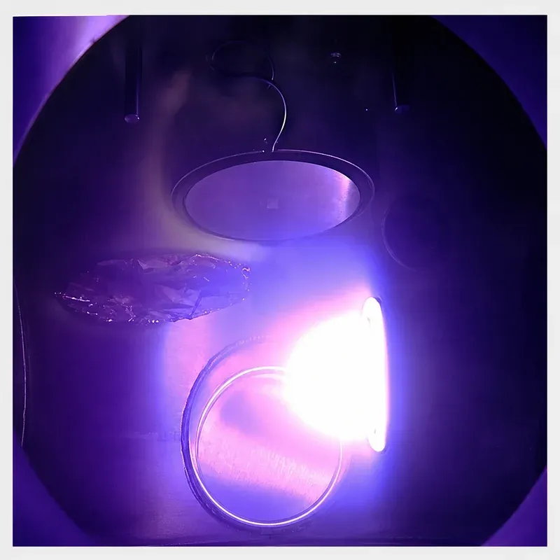
VanaM combines proprietary sputtering/ALD processes, pre- and post-treatment, in-situ process sensing, and thin film metrology to develop high-quality materials with faster optimization cycles and stronger process reproducibility.
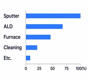
Data collection
ALD

Sputter

Measurement

Data Integration & Preprocessing
A. Data Integration Repository

- · Raw data storage
- · Time synchronization
- · Metadata mapping
B. Preprocessing & Quality Validation

- · Data Validation
- · Outlier Filtering
- · Missing Value Check
- · Measurement Quality Assessment
✓ Data quality
Multivariate Analysis & Change Detection
A. Integrated Monitoring Dashboard
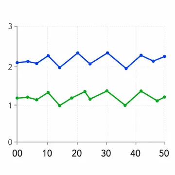
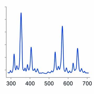
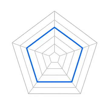
B. Change Detection (Early Anomaly Detection)
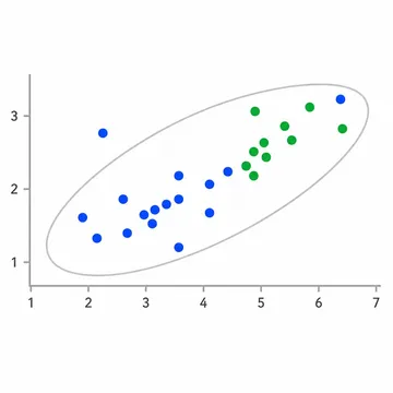
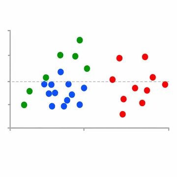
Alarm Level
Normal
Stable pattern
Continuous monitoring
Warning
Minor change
Trend observation
Critical
Significant change
Cause analysis
Diagnosis & Cause Estimation

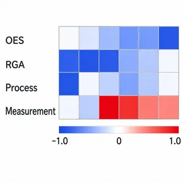
Diagnosis result
Identify the key factors and main causes of the process condition change
Decision & Action
Action Execution (Feedback)Decision making

Condition Adjustment
Power / Pressure / Temperature …

Recipe modification
Pulse / Purge / Sequence …

Maintenance
Inspection / Cleaning

Additional experiment
DOE
Conduct experiment
- · Execute selected action immediately
- · Or apply to the next lot
Verification & Learning
Effect verification
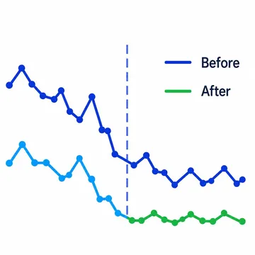
Verify Metric improvement
- · Electrical Properties
- · TMI / dT / TCR Stabilization
- · Reproducibility / Yield
Standardization & Documentation
- · Optimal Condition Update
- · Recipe Standardization

Continuous improvement loop
↻ Feedback loop 5 → 1
CORE VALUE
Early Detection → Fast Action → Better Result
 Early detection
  Fast diagnosis
  Accurate control
  Continuous optimization
  Final goal
 High yield & Reproducibility · Minimize process variation · Data-driven smart factory realization
THE QUANTUM PHOTONICS PROJECT
Thin films for next-generation PICs and quantum systems
VanaM is developing the major thin-film building blocks needed for cryogenic photonic integrated circuits and quantum hardware, with collaboration pathways including KIST Quantum Fab and UIUC.
SNSPD
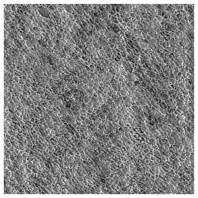
NbTiN / NbN films for high-sensitivity single-photon detection.
Waveguides
Ta₂O₅, SiN and TiO₂ films for low-loss optical waveguides.
Modulators
BTO and STO thin films for cryogenic electro-optic modulation.
DBR Mirrors
Si, SiO₂, TiO₂ and Ta₂O₅ multilayer stacks for high-reflectance mirrors.
SNSPD
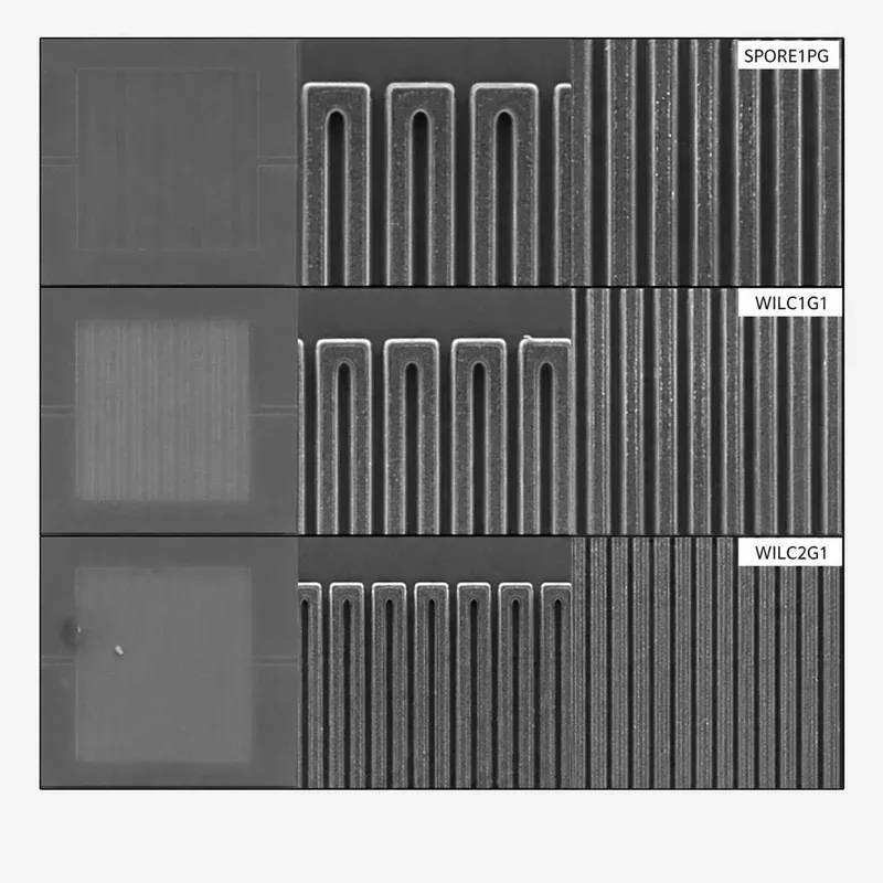
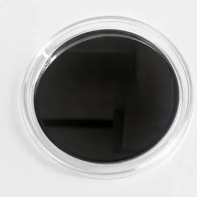
High-sensitivity superconductors
Waveguide
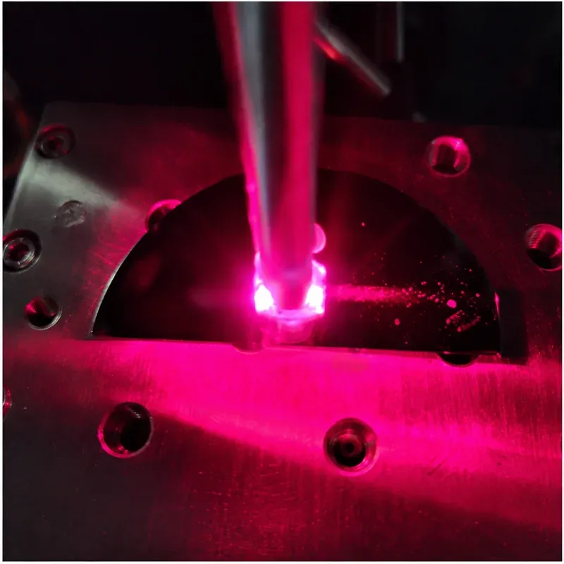
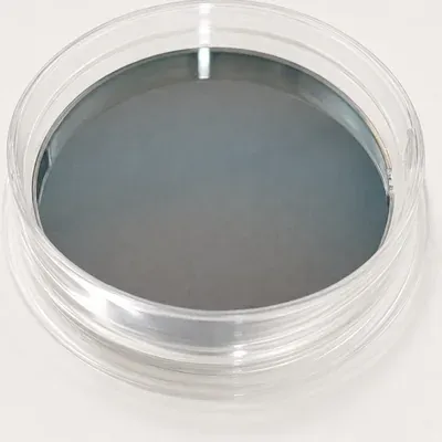
Low loss optical waveguides
Modulator
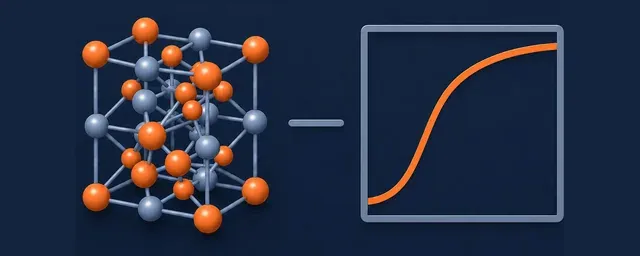
High cryogenic electro-optic modulation
DBR
High-reflection DBR wafer
Photonics Integrated Circuits (PIC)
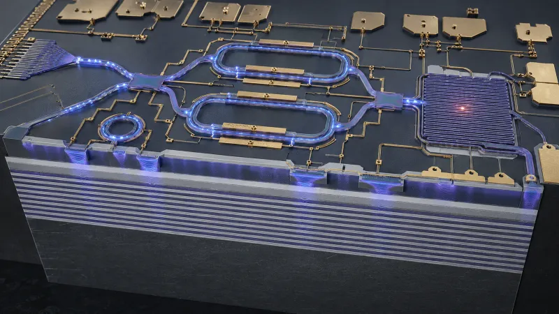
Key Thin Films for Next-Gen PICs & Quantum Systems
- SNSPD: NbTiN
- Waveguide: Ta₂O₅
- Modulator: BTO, STO
- DBR: Si-SiO₂-TiO₂
- ✓Superconducting transition T ~ 11K
- ✓Propagation loss < 0.5 dB
- ✓Pockels coefficient ~1000 pm/V at 5K
- ✓Reflectance > 99%

KIST Quantum Fab & UIUC Collaboration
Scalable Opportunities / Areas
Quantum Computers

$13 Bn
CAGR 32%
Quantum Communication

$12 Bn
CAGR 30%
Quantum Sensors

$1.6 Bn
CAGR 26%
Laser & LiDAR

$22 Bn
CAGR 30%
Glass Core Substrate

$223 Bn
CAGR 8%
Silicon Photonics

$1.9 Bn
CAGR 17%
Source: MarketsandMarkets, MMR, Precedence Research, Fact.MR
Target applications
THE MULTIFUNCTIONAL ENERGY-RESPONSIVE SEMICONDUCTOR PROJECT
Multifunctional VO₂ thin films that sense, respond, and protect.
VanaM developed the world's first multifunctional semiconductor thin-film that responds to changes in thermal and electrical energy, enabling sensing, switching, protection, and energy-management functions to be integrated into compact devices and surfaces.
Thermal & Electrical Sensing & Smart Switching
Energy-responsive thin films that detect changes in temperature and electrical conditions for real-time sensing and monitoring.
One Thin Film, Multiple Functions
Multifunctional thin film that can replace several traditional active and passive components, for simplified, less energy-consuming systems.
Safety & Protection
Responsive thin films for early heat and abnormal-condition detection, supporting applications such as fire detection and electronic system protection.
Energy Management
Functional coatings that help control heat, light, and energy flow for more efficient buildings, electronics, and intelligent surfaces.
From Bulk Components
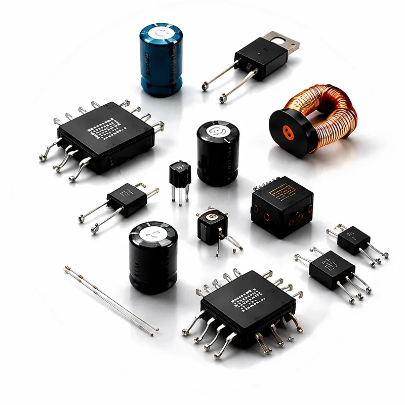
To A Single Thin Film
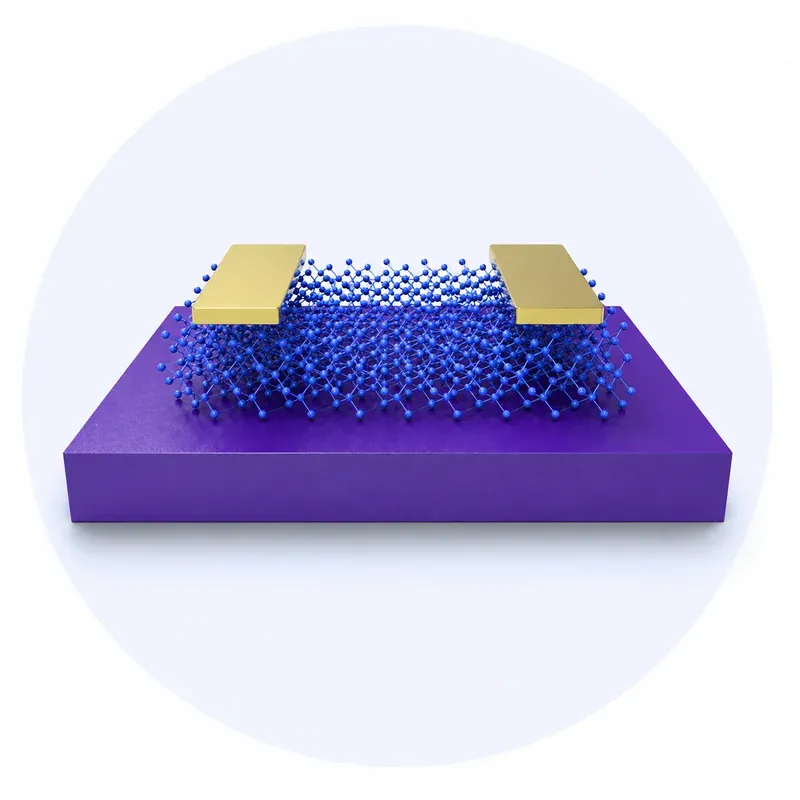
Extra Sensory

Sensitive to heat and electrical energy
Super Safe

Passive & active components into a single thin film
Key Thin Film Benefits

Sensitive to heat and electrical energy

Passive & active components into one thin film

Enhanced accuracy, lightweight system, lower-power operation

Applications: Thermal management & control systems, protection circuits
Scalable Opportunities / Areas
IR Image Sensing

$8 Bn
Military (Stealth)

$42 Bn
Smart Glass

$15 Bn
AI Semiconductors

$123 Bn
Power Electronics

$50 Bn
Energy Storage

$256 Bn
Source: MarketsandMarkets, MMR, Precedence Research, Fact.MR
Target applications
PROCESS AUTOMATION
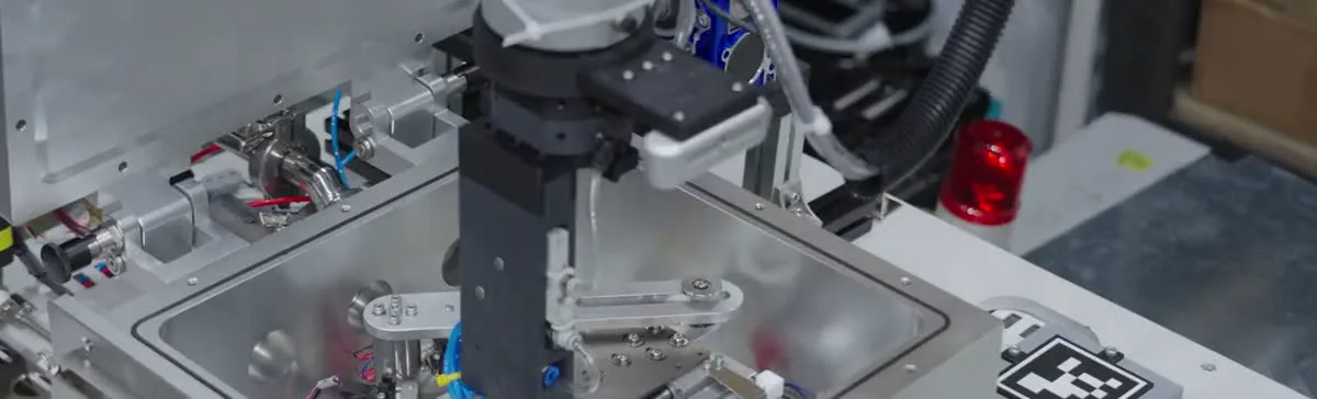
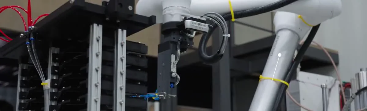
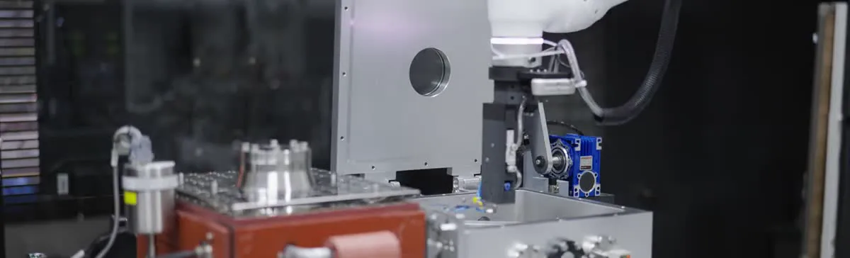
A deposition line that runs without hands on it
Robots take over from wafer loading through chamber transfer and process changeover. The line keeps running at night and on weekends, so the same equipment handles more samples — and with fewer points of human contact, contamination and run-to-run variation drop as well.
Have a thin-film challenge?
Tell us your target material or process — we'll help you get there faster.
Talk to us