

Products
Thin films,
off the shelf
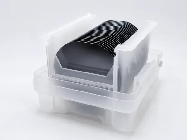
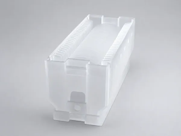
Order standard samples and services directly. For custom deposition, request a quote and we'll price it for you.
No account needed — checkout as a guest.
How a deposition order works
From your specifications to a film in your hands.
- 01
Request
Tell us the material, substrate and process conditions you need.
- 02
Expert review
Our team checks feasibility and pre-/post-process requirements.
- 03
Quotation
We send a price and lead time for your exact specifications.
- 04
Deposition
We run the process on our own equipment, collecting process data throughout.
- 05
Quality check
Basic inspection before shipping. Further analysis available on request.
- 06
Shipping
The film ships to you. Device fabrication can follow if needed.
Analysis & Measurement Solution
From non-destructive spectroscopy to electrical characterisation.
Material analysis
- SEM (include EDS) Scanning electron microscopy
- TEM (include EDS) Transmission electron microscopy
- XRD X-ray diffraction — crystallinity
- XPS X-ray photoelectron spectroscopy
- UPS UV photoelectron spectroscopy
- AFM Atomic force microscopy
- Raman Raman spectroscopy
Device characterisation
- I–V Current–voltage characteristics
- C–V Capacitance–voltage characteristics
- Pulse Pulse measurement
- Ferroelectric Polarisation hysteresis
- Piezoelectric Piezoresponse measurement
- Hall Hall effect measurement
- PPMS Physical property measurement system (2 K ~ 400 K)
Equipment Solution
Deposition tools built in-house with vacuum specialists of 30+ years — every one of them instrumented for process data.
PVD & ALD
Sputtering, thermal evaporator, in-line sputter, 6-inch and 12-inch ALDs
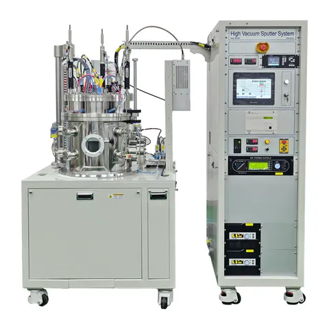
Sputter
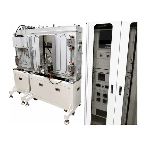
In-line Sputter
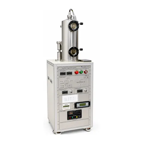
Thermal Evaporator
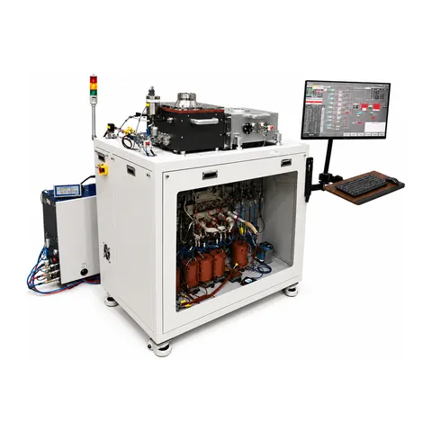
ALD — 6-inch
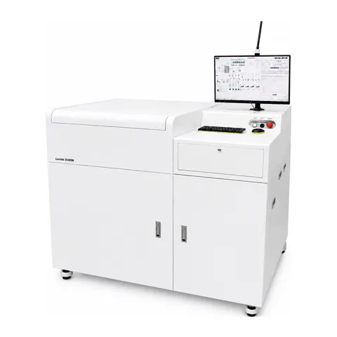
ALD — 12-inch
Process Big Data Collection System
In-situ collection of plasma emission, residual gas, and key process parameters. The collected data supports machine-learning-based process optimization and material-property prediction.
01 IN-SITU SENSING Self-developed sputter · 3 real-time sensors
02 BIG DATA + AI Collection · training · analysis
03 OUTCOMES Optimization · prediction
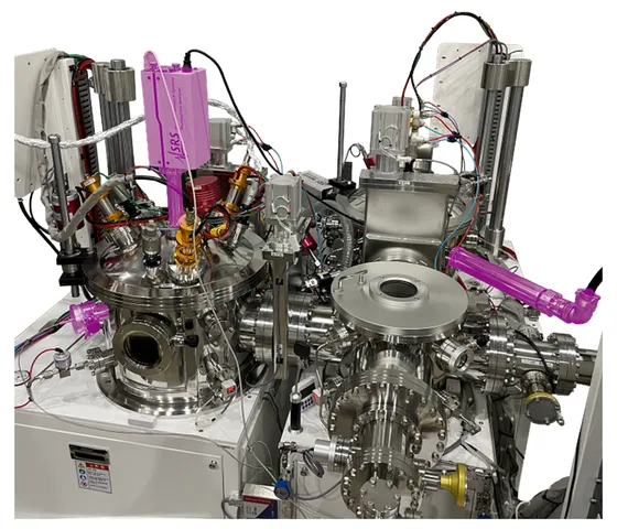
Self-developed Sputter
RGA — Residual Gas Analyzer · OES — Optical Emission Spectrometer · TSP — Titanium Sublimation Pump
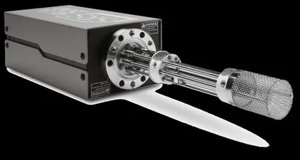
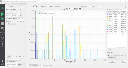
RGA — analyzer · measured spectrum
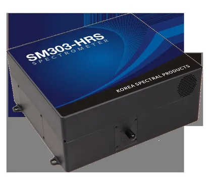
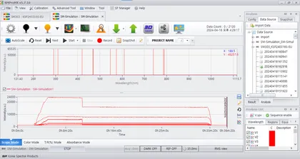
OES — spectrometer · emission spectrum
Big Data + AI
Process-data collection · machine-learning training
Process Optimization
Thin film process optimization
Property Prediction Model
Characteristic prediction model